QS-KI-OUT4-REVA · Rev-A · KI-OUT4-RevA / PCBV1.01
OUT-4 Quick Start Guide
In seven steps
Wire one supply, share ground with the controller, then switch one load at a time.
- 5–24 VDC load supply
- 4 low-side MOSFET outputs
- 1.0 A continuous per channel
- 3.3 V / 5 V logic · HIGH = ON
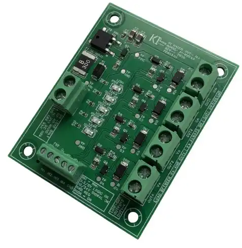
This board is for
- LED strips, relays, and solenoids within the 1.0 A published rating
- Arduino, ESP32, or Raspberry Pi GPIO that should not drive the load directly
- Applications where per-channel visual output indication is useful.
This board is not
- Isolated outputs or relay contacts
- A 10 A module — published continuous rating is 1.0 A per channel
- AC mains, or a motor driver / H-bridge
- A safety, e-stop, medical, or fail-safe output
Read before power-up
- Use 5–24 VDC on CN1. 30 VDC absolute maximum. No AC mains anywhere on the board.
- V+ is always on. OUTx pulls the load negative to ground. These are not isolated relay contacts.
- Wire each load on its own 2-pin block: load + to V+, load − to OUTx. Do not return the load to DC−.
- CN2 GND must be common with the microcontroller ground. No GND return means the MOSFET stays off.
- Not a safety or e-stop output. No isolation, no per-channel fuse, no certified safe-off path.
5-minute first power-up
- Inspect the silkPower on the left (CN1 DC+ / DC−). Logic along the bottom (IN1–IN4, GND). Four V+ / OUTx load blocks on the right.
- Mount the boardInsulated M3 standoffs. Keep the bottom side away from conductive surfaces, loose hardware, and debris.
- Wire the DC supply only5–24 VDC into CN1. DC+ upper screw, DC− lower. Leave controller and loads off for this check.
- Confirm PWR OKLED1 should light. If it does not, stop and verify input polarity, supply voltage, and the condition of F1 before connecting a load.
- Share ground, then one GPIOCN2 GND to MCU GND. MCU output to IN1 as OUTPUT. HIGH = ON. 3.3 V is enough.
- Wire one load on CN3Load + to V+. Load − to OUT1. Never to DC−. For inductive loads, use the paired V+ and OUTx terminals so the onboard flyback protection is connected across the load.
- Drive IN1 HIGH, then add channelsLED2 (OUT1 ON) lights and the load turns on. Repeat on CN4–CN6. Remember that all four channels share the board’s 3 A total current limit through F1.
Expected first-use result
PWR OK on. IN1 HIGH turns OUT1 and the CN3 load on. IN1 LOW turns it off. At lower supply voltages, the channel indicator LEDs may appear less bright; this is expected. Then add one channel at a time.
Most important wiring rule
OUT1–OUT4 are low-side switches
Connect the load positive wire to that channel’s V+ screw and the load negative wire to OUTx. V+ is always on. OUTx switches the negative.
Do not wire OUTx like a floating relay contact. Do not return the load to DC−. For inductive loads, use the paired V+ and OUTx terminals so the onboard flyback protection is connected across the load.
Connector groups
| Connector | Quick use |
|---|---|
| CN1 DC+ / DC− | 5–24 VDC load supply. 30 VDC absolute maximum. Check polarity before a load is attached. |
| CN2 IN1–IN4 + GND | 3.3 V / 5 V logic. HIGH = ON. Common ground with the controller is required. |
| CN3 V+ / OUT1 | Channel 1 load pair. Load + to V+, load − to OUT1. |
| CN4 V+ / OUT2 | Channel 2 load pair. |
| CN5 V+ / OUT3 | Channel 3 load pair. |
| CN6 V+ / OUT4 | Channel 4 load pair. |
Released ratings
Published continuous rating is 1.0 A per channel, 3 A board total through shared fuse F1. Channels are not short-circuit protected.
| Parameter | Limit |
|---|---|
| Load supply (CN1) | 5–24 VDC nominal · 30 VDC absolute maximum |
| Outputs | 4 independent low-side N-MOSFET switches |
| Per channel | 1.0 A continuous · not short-circuit protected |
| Board total | 3 A hold through shared PPTC fuse F1 |
| Logic inputs | 3.3 V / 5 V logic · HIGH = ON · common ground required · not isolated |
| PWM | Suitable for switching and low-frequency PWM; verify MOSFET and connector temperature for the intended load and duty cycle. |
| Mechanical | 65.00 × 50.00 mm board · 55.00 × 40.00 mm mounting · 4× Ø3.20 mm M3 |
Thermal / current
Verify MOSFET temperature, connector temperature, and enclosure airflow during first tests — especially above 500 mA or with slow PWM.
Stop immediately if…
- You are about to connect AC power, an AC-output adapter, or any source above 30 VDC to CN1.
- You are not sure the load is between that channel’s V+ and OUTx, or whether CN2 GND is common with the controller.
- PWR OK does not light, a channel LED pattern seems wrong, or a MOSFET, fuse, or connector becomes unexpectedly hot.
What to read next
Kuster Induction Solutions LLC · KI Maker OUT-4 Rev-A · PCBV1.01 · QS-KI-OUT4-REVA · Low-voltage DC only · Not for AC mains, life-safety, medical, or certified safety systems.
QS-KI-OUT4-REVA · Rev-A · KI-OUT4-RevA / PCBV1.01
OUT-4 Quick Start Guide
In seven steps
Wire one supply, share ground with the controller, then switch one load at a time.
- 5–24 VDC load supply
- 4 low-side MOSFET outputs
- 1.0 A continuous per channel
- 3.3 V / 5 V logic · HIGH = ON
This board is for
- LED strips, relays, and solenoids within the 1.0 A published rating
- Arduino, ESP32, or Raspberry Pi GPIO that should not drive the load directly
- Applications where per-channel visual output indication is useful.
This board is not
- Isolated outputs or relay contacts
- A 10 A module — published continuous rating is 1.0 A per channel
- AC mains, or a motor driver / H-bridge
- A safety, e-stop, medical, or fail-safe output
Read before power-up
- Use 5–24 VDC on CN1. 30 VDC absolute maximum. No AC mains anywhere on the board.
- V+ is always on. OUTx pulls the load negative to ground. These are not isolated relay contacts.
- Wire each load on its own 2-pin block: load + to V+, load − to OUTx. Do not return the load to DC−.
- CN2 GND must be common with the microcontroller ground. No GND return means the MOSFET stays off.
- Not a safety or e-stop output. No isolation, no per-channel fuse, no certified safe-off path.
5-minute first power-up
- Inspect the silkPower on the left (CN1 DC+ / DC−). Logic along the bottom (IN1–IN4, GND). Four V+ / OUTx load blocks on the right.
- Mount the boardInsulated M3 standoffs. Keep the bottom side away from conductive surfaces, loose hardware, and debris.
- Wire the DC supply only5–24 VDC into CN1. DC+ upper screw, DC− lower. Leave controller and loads off for this check.
- Confirm PWR OKLED1 should light. If it does not, stop and verify input polarity, supply voltage, and the condition of F1 before connecting a load.
- Share ground, then one GPIOCN2 GND to MCU GND. MCU output to IN1 as OUTPUT. HIGH = ON. 3.3 V is enough.
- Wire one load on CN3Load + to V+. Load − to OUT1. Never to DC−. For inductive loads, use the paired V+ and OUTx terminals so the onboard flyback protection is connected across the load.
- Drive IN1 HIGH, then add channelsLED2 (OUT1 ON) lights and the load turns on. Repeat on CN4–CN6. Remember that all four channels share the board’s 3 A total current limit through F1.
Expected first-use result
PWR OK on. IN1 HIGH turns OUT1 and the CN3 load on. IN1 LOW turns it off. At lower supply voltages, the channel indicator LEDs may appear less bright; this is expected. Then add one channel at a time.
Most important wiring rule
OUT1–OUT4 are low-side switches
Connect the load positive wire to that channel’s V+ screw and the load negative wire to OUTx. V+ is always on. OUTx switches the negative.
Do not wire OUTx like a floating relay contact. Do not return the load to DC−. For inductive loads, use the paired V+ and OUTx terminals so the onboard flyback protection is connected across the load.
Connector groups
| Connector | Quick use |
|---|---|
| CN1 DC+ / DC− | 5–24 VDC load supply. 30 VDC absolute maximum. Check polarity before a load is attached. |
| CN2 IN1–IN4 + GND | 3.3 V / 5 V logic. HIGH = ON. Common ground with the controller is required. |
| CN3 V+ / OUT1 | Channel 1 load pair. Load + to V+, load − to OUT1. |
| CN4 V+ / OUT2 | Channel 2 load pair. |
| CN5 V+ / OUT3 | Channel 3 load pair. |
| CN6 V+ / OUT4 | Channel 4 load pair. |
Released ratings
Published continuous rating is 1.0 A per channel, 3 A board total through shared fuse F1. Channels are not short-circuit protected.
| Parameter | Limit |
|---|---|
| Load supply (CN1) | 5–24 VDC nominal · 30 VDC absolute maximum |
| Outputs | 4 independent low-side N-MOSFET switches |
| Per channel | 1.0 A continuous · not short-circuit protected |
| Board total | 3 A hold through shared PPTC fuse F1 |
| Logic inputs | 3.3 V / 5 V logic · HIGH = ON · common ground required · not isolated |
| PWM | Suitable for switching and low-frequency PWM; verify MOSFET and connector temperature for the intended load and duty cycle. |
| Mechanical | 65.00 × 50.00 mm board · 55.00 × 40.00 mm mounting · 4× Ø3.20 mm M3 |
Thermal / current
Verify MOSFET temperature, connector temperature, and enclosure airflow during first tests — especially above 500 mA or with slow PWM.
Stop immediately if…
- You are about to connect AC power, an AC-output adapter, or any source above 30 VDC to CN1.
- You are not sure the load is between that channel’s V+ and OUTx, or whether CN2 GND is common with the controller.
- PWR OK does not light, a channel LED pattern seems wrong, or a MOSFET, fuse, or connector becomes unexpectedly hot.
What to read next
Kuster Induction Solutions LLC · KI Maker OUT-4 Rev-A · PCBV1.01 · QS-KI-OUT4-REVA · Low-voltage DC only · Not for AC mains, life-safety, medical, or certified safety systems.